Conventional semiconductor light sources generate photons in an active layer; however, their efficient excitation is technically challenging. The invention solves this problem by employing a ring-shaped pump section with an integrated inner active layer, thereby enabling resonant coupling. This allows more of the generated photons to be utilised, and the generation process is more targeted and reliable. Monolithic integration on a single chip also allows for a compact design and facilitates integration into larger systems, as well as precise wavelength control. Overall, the technology enables the efficient, low-loss and controlled generation of single photons and is therefore particularly relevant for applications in quantum communication, quantum cryptography and quantum computing.
Due to the potential for monolithic integration, the technology is particularly well-suited for compact semiconductor light sources and integrated photonic platforms based on compact, electrically driven single-photon sources. Photons can be generated and utilised in a more targeted and reliable manner, with high indistinguishability and lower loss. This makes them particularly interesting for new technologies in quantum communication, quantum cryptography and future quantum computers, where high efficiency and control over individual photons with excellent quantum properties are crucial.
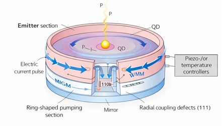
Conventional semiconductor light sources emit photons as a result of an emission process within an active layer. However, efficiently exciting this layer presents a technical challenge, particularly when electrical operation is to be combined with resonant effects for the generation of indistinguishable single photons.
The present invention addresses this challenge by combining a ring-shaped pump section with an inner active layer arranged within this structure, thereby enabling resonant coupling of the pump radiation. More of the photons generated can actually be used instead of being lost in an uncontrolled manner. The special resonator structure increases the probability that a photon will be generated exactly when it is needed. Since the pump and emitter areas are integrated on a common semiconductor chip, the technology is easier to miniaturise and integrate into larger systems. The new structure allows active fine control of the excitation and emission wavelengths, and the number of useful photons per excitation process can be increased.
Ina Krüger
Technology Transfer Manager
+49 (0)30 314-75916
ina.krueger@tu-berlin.de
Experimental proof of concept
pending: DE, EP, US
Technische Universität Berlin
The Center for Intellectual Property (ZfgE) at the TU Berlin is the central point of contact for all topics relating to intellectual property law and intellectual property.
We patent and market the inventions of the TU Berlin, and we also teach and research technical and intellectual property law.
This makes us the central contact for inventors of the TU Berlin, for cooperation partners from industry and science as well as for interested scientists and experts from the fields of technology and law.
Zentrum für geistiges Eigentum
Technische Universität Berlin
Straße des 17. Juni 135
10623 Berlin