Background
In the field of heavy-wire bonding (using wires with diameters between approximately 100 μm and approximately 500 μm), the different thermal expansion coefficients of the materials involved – in particular of the semiconductor and the heavy wire – lead to fatigue cracks forming in the contacting plane of the heavy-wire bond connections. Therefore, technologies are needed to prevent this problem in heavy-wire bond connections.
Technical Description
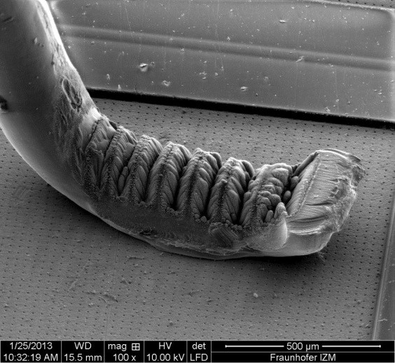
This invention comprises a heavy-wire bond arrangement which comprises a substrate, a heavy wire and a high-voltage heavy-wire bond connection.
In this connection one end bond section of the heavy wire is bonded with the substrate. Here, the section extends towards the end of the heavy wire, so that a bond contact between and the substrate is formed in the area of the bond section.
The heavy wire has a tapering section which adjoins the end of the wire. In this tapering section, the wire cross-section tapers towards the end of the wire.
The provision of the tapering section, which in the bond section extends from the heavy wire so far that it reaches the end of the wire, reduces the effective shear stress in the area of the bond section, resulting in an improved reliability of the bond connection between heavy wire and substrate. Moreover, the likelihood of fatigue cracks is reduced and the current-carrying capacity is maintained in the area of the bond section.
First Results
It could be shown that tapering the end of the wire reduces the stress in the interface as well as the accumulated distention and the tensions inside the tail area and the heel area.
Possible Applications
The technology can be used in the construction of electrical connections. Typically wire bonding is used for connecting a so-called die to electrical connections of a chip housing, like for example the semiconductors of an integrated semiconductor, a light emitting diode or a sensor.
Laser-structured adhesive sections, the chip remains functional.
