Background
Today, transmission electron microscopy (TEM) is the main technique used to investigate materials in the nanometer range (semiconductor devices, processors, functional materials). Electron holography, as an extension, allows the measurement of electric and magnetic fields with the same spatial resolution. For this the interference pattern of two superimposed electron beams is recorded over a given exposure time and evaluated. In the TEM, it is technically very demanding to lower recording times beneath the millisecond range and thus to investigate dynamic processes.
Technical Description
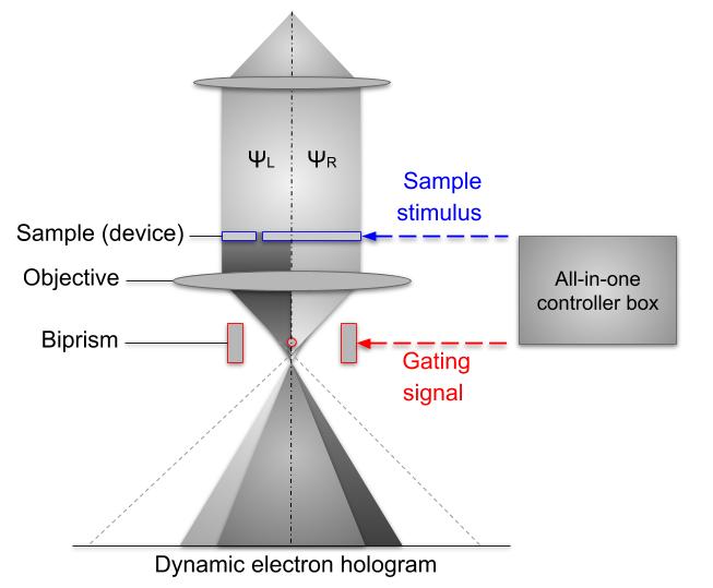
The presented invention describes how the exposure time of almost any TEM can be significantly increased with minimal technical effort. For this purpose, the interference pattern is intentionally disturbed for a certain time within the exposure time and remains undisturbed for a fraction of the exposure time. The entire measured interference pattern is holographically reconstructed, whereby only the information from the undisturbed time range, which is much shorter than the exposure time, is filtered out. This allows time resolutions in the nano- and picosecond range with spatial resolutions in the nanometer range.
Possible Applications
Investigation of dynamic processes in semiconductor structures (switching processes of transistors in computer chips), Investigation of nanostructures (2-D materials, nanotubes, nanowires)
Simplified setup of the experiment.
