The pre-patterning of a surface to obtain locally arranged nanostructures is usually achieved by using complex patterning techniques like the electron beam lithography, the focused ion beam etching or the ion implantation. But such direct surface patterning techniques can cause crystal damages and defects, thus reducing the quality and the performance of the nanostructured elements. Other disadvantages are that these techniques only have a short-range impact and that they are not fit for batch processing.
Technical Description
A method for fabricating layer assemblies with locally arranged nanostructures is provided by this invention from TU Berlin. A buried, selectively modified underlying layer is used to control the growth of nanostructures on the surface by controlling the laterally inhomogeneous strain distribution. This is done using standard lithography, etching and oxidation techniques.
Possible Applications
With this method light emitting devices can be built as well as single photon emitters. It also enables quantum cryptography and quantum communication.
Potential Industries: Lighting, Information Technology Nanoelectronics, Security Industry
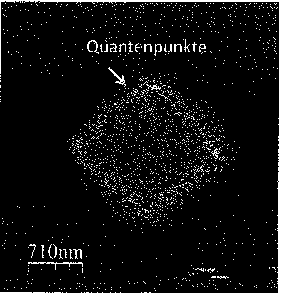
Shows the strain induced formation of QD
Benefits
Long-range impact
No defects in close vicinity of the nanostructures
Use of conventional structuring methods
[...] further benefits online
Technology Readiness Level
Experimental proof of concept (TRL: 3)