Background
Transmission electron microscopy (TEM) is the preferred tool for investigating materials and electronic devices, as needed in the semiconductor technology, at the nanometer scale. Electron holography, as an extension, allows the measurement of electronic and magnetic field magnitudes in the TEM with the same spatial resolution. Typical electronic measurement techniques, such as oscillography, which always investigate a complete electronic system lack exactly this local information.
Technical Description
The presented method allows measurements of electronic processes with high spatial resolution. By combining a time-resolved electron holographic evaluation of the phase, conclusions can be drawn about the dynamic behavior of nanodevices and their causes, like capacitances. In this context, possible boundary effects, like surface or interface effects, can be investigated simultaneously by means of location-dependent measured value formation.
Possible Applications
Investigation of dynamic processes in semiconductor structures (switching processes of transistors in computer chips, investigation of nanostructures (2D-materials, nanotubes, nanowires).
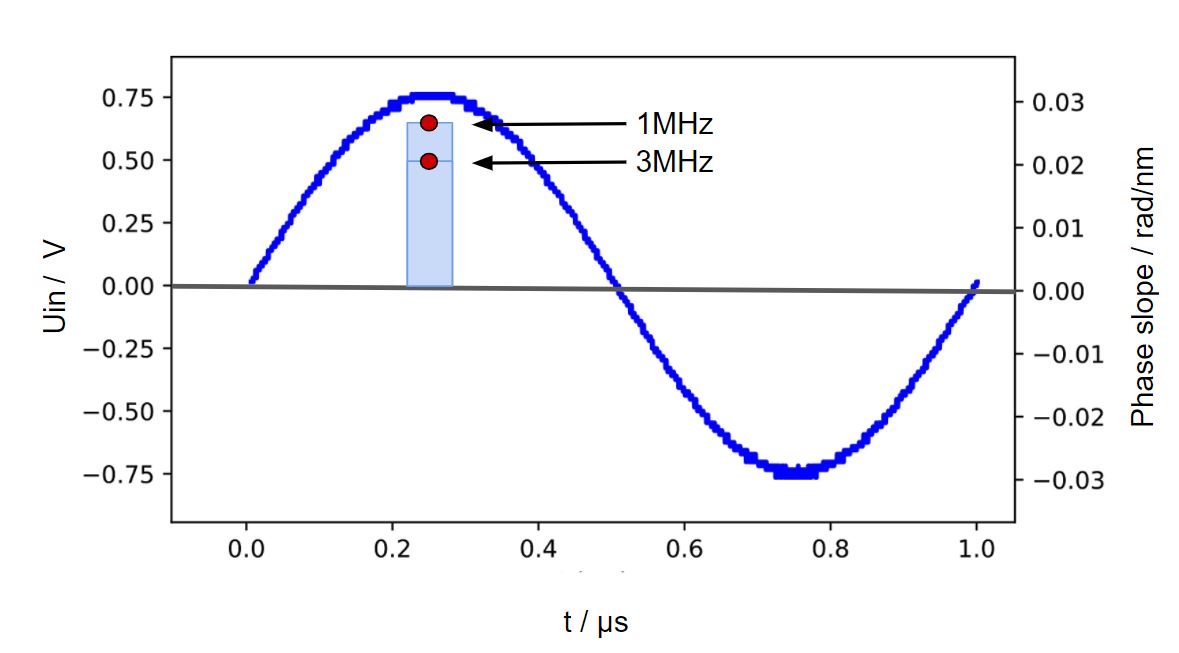
Figure: Change of the measured phase slope at a certain location of the device. Exemplary the AC voltage applied to the component with a frequency of 1 MHz (blue), the signal at 3 MHz is not shown. (© TU Berlin)
