This innovative memory cell offers both high performance and long life and can be used in the computer industry, optoelectronics or consumer electronics.
The presented memory cell is suitable for opto-electronic devices and for data storage. Computer industry, optoelectronics, consumer electronics
Computer data storage can be classified into volatile and non-volatile storage. Volatile memories like dynamic random access memories (DRAMs) are short-term memories with a high writing speed, but they require an external power source for data storage – whereas non-volatile flash memories do not need an external power source and are able to store data for years, but they write information about 1000 times slower than DRAMs.
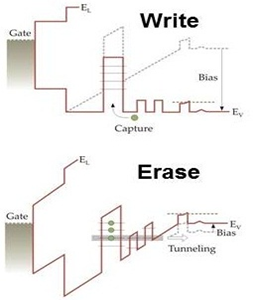
Our novel semiconductor nanostructure based memory cell combines the advantages of the non-volatility of flash memories with the performance and the endurance of a DRAM. The memory comprises a strained double heterostructure, has an inner semiconductor layer comprising quantum dots and is sandwiched by two outer semiconductor layers. The memory cell uses holes as charge carriers.
Ina Krüger
Technology Transfer Manager
+49 (0)30 314-75916
ina.krueger@tu-berlin.de
Experimental proof of concept
approved: US, JP, DE, FR, GB, IE, KR
Technische Universität Berlin
The Center for Intellectual Property (ZfgE) at the TU Berlin is the central point of contact for all topics relating to intellectual property law and intellectual property.
We patent and market the inventions of the TU Berlin, and we also teach and research technical and intellectual property law.
This makes us the central contact for inventors of the TU Berlin, for cooperation partners from industry and science as well as for interested scientists and experts from the fields of technology and law.
Zentrum für geistiges Eigentum
Technische Universität Berlin
Straße des 17. Juni 135
10623 Berlin