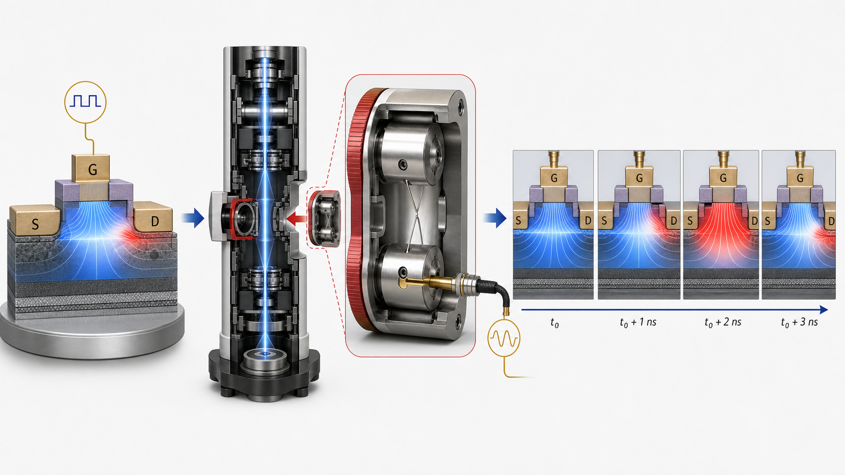
Dynamic electrical processes in semiconductor devices and nanostructures are too fast for conventional transmission electron microscopes (TEM). Existing time-resolved electron-holography approaches require specialised modifications. This retrofit-ready module brings nanosecond phase-sensitive imaging to established TEM platforms while retaining static electron holography.
The module upgrades compatible conventional TEMs for nanosecond time-resolved TEM and electron holography while preserving static operation. Applications include dynamic potential mapping in semiconductor devices, operando studies of functional nanostructures and high-frequency electron-wave control. Commercial routes include licensing, OEM integration and joint development with TEM manufacturers and accessory suppliers.
Conventional techniques using transmission electron microscopy (TEM) offer very high spatial resolution, but are limited in terms of time when it comes to rapidly occurring processes. To investigate dynamic processes in semiconductors and nanostructures, the information must therefore be recorded not only spatially but also at defined points in time. Time-resolved electron holography combines the high spatial resolution of electron microscopy with precise temporal control of the interference signal.
The patented module combines an electron biprism with a high-frequency control electrode integrated into one counter electrode. A low-loss coaxial RF feed enables rapid, precise modulation of the electron-wave phase. Designed for a conventional TEM aperture holder, the module can be installed by holder exchange without extensive microscope modification.
The integrated electrode controls the electron-wave phase. The coaxial feed is designed for 5 kHz to 50 GHz, with preferred operating voltages from 10 kHz to 1 GHz. Several geometries enable application-specific field shaping.
Ina Krüger
Technology Transfer Manager
+49 (0)30 314-75916
ina.krueger@tu-berlin.de
System prototype demonstration in operational environment
pending: EP, US
Technische Universität Berlin


The Center for Intellectual Property (ZfgE) at the TU Berlin is the central point of contact for all topics relating to intellectual property law and intellectual property.
We patent and market the inventions of the TU Berlin, and we also teach and research technical and intellectual property law.
This makes us the central contact for inventors of the TU Berlin, for cooperation partners from industry and science as well as for interested scientists and experts from the fields of technology and law.
Zentrum für geistiges Eigentum
Technische Universität Berlin
Straße des 17. Juni 135
10623 Berlin