Conventional high-power lasers often have poor beam quality. The invention addresses this problem through the an unique spatial layer design and refractive index profile defining the waveguide.
The invention paves the way for single mode high brightness lasers (cw and pulsed) used in optical communication, material processing, sensor technology, and for medical and scientific laser systems. Further applications include fibre-coupled laser modules, integrated photonic components and pump sources for solid state or fiber lasers. Due to the improved beam quality, the technology is particularly relevant for systems that need to combine high brightness with inexpensive beam shaping.
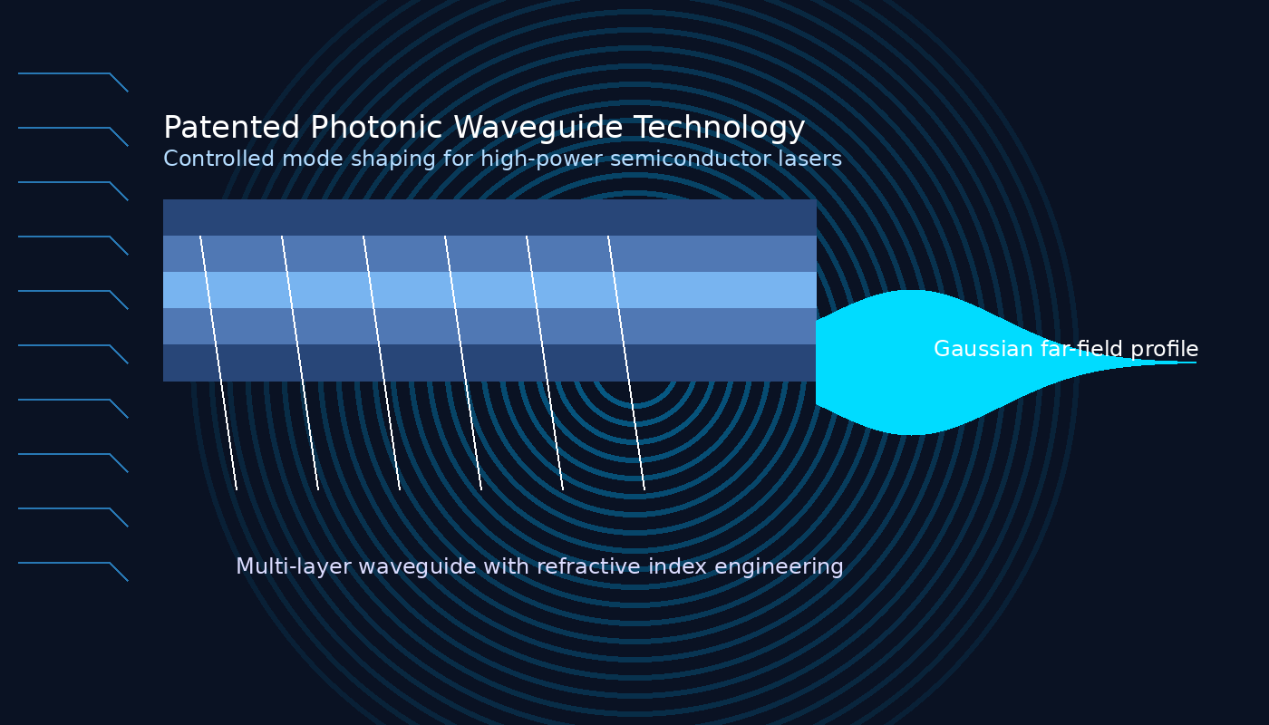
Conventional high-power lasers often exhibit poor beam quality because multiple transverse modes are excited simultaneously. This results in complex near-field profiles and broad far-field distributions. Existing approaches to mode control often cause additional losses or limit the maximum achievable output power. The invention addresses this problem through the targeted spatial design of the refractive index profiles within the waveguide.
The device comprises a waveguide with several layers of varying refractive indices. At least one layer has a refractive index that varies across its thickness. This results in controlled coupling between transverse modes. The patent specification describes various embodiments with single or multiple low- or high-refractive-index layers, as well as periodic structures. Several figures demonstrate that unwanted secondary maxima in the near field can be suppressed whilst simultaneously generating a single intense far-field maximum. Additionally, designs incorporating integrated gain regions, pump sources and resonator structures are described.
The technology can be used in both semiconductor lasers and other integrated optical components.
Ina Krüger
Technology Transfer Manager
+49 (0)30 314-75916
ina.krueger@tu-berlin.de
Technology validated in lab
approved: US
Technische Universität Berlin
The Center for Intellectual Property (ZfgE) at the TU Berlin is the central point of contact for all topics relating to intellectual property law and intellectual property.
We patent and market the inventions of the TU Berlin, and we also teach and research technical and intellectual property law.
This makes us the central contact for inventors of the TU Berlin, for cooperation partners from industry and science as well as for interested scientists and experts from the fields of technology and law.
Zentrum für geistiges Eigentum
Technische Universität Berlin
Straße des 17. Juni 135
10623 Berlin