With this method, light emitting devices as well as single photon emitters can be constructed by producing layers with locally arranged nanostructures, and quantum cryptography and communication are also made possible.
With this method light emitting devices can be built as well as single photon emitters. It also enables quantum cryptography and quantum communication. Potential Industries: Lighting, Information Technology Nanoelectronics, Security Industry
The pre-patterning of a surface to obtain locally arranged nanostructures is usually achieved by using complex patterning techniques like the electron beam lithography, the focused ion beam etching or the ion implantation. But such direct surface patterning techniques can cause crystal damages and defects, thus reducing the quality and the performance of the nanostructured elements. Other disadvantages are that these techniques only have a short-range impact and that they are not fit for batch processing.
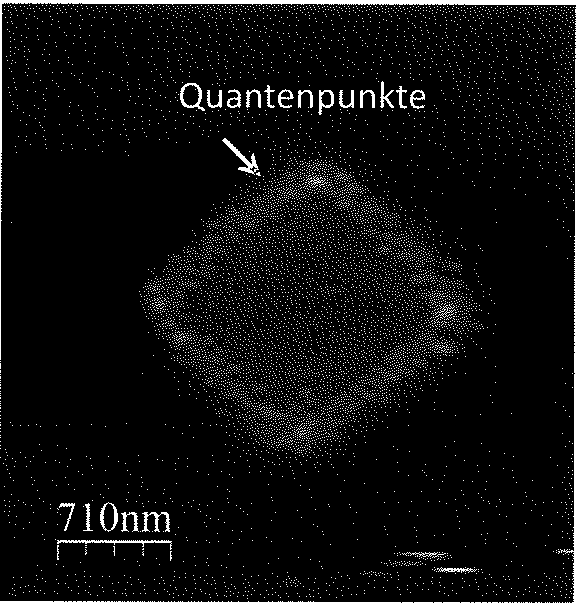
A method for fabricating layer assemblies with locally arranged nanostructures is provided by this invention from TU Berlin. A buried, selectively modified underlying layer is used to control the growth of nanostructures on the surface by controlling the laterally inhomogeneous strain distribution. This is done using standard lithography, etching and oxidation techniques.
Ina Krüger
Technology Transfer Manager
+49 (0)30 314-75916
ina.krueger@tu-berlin.de
Experimental proof of concept
approved: US, DE, FR, GB
Technische Universität Berlin
The Center for Intellectual Property (ZfgE) at the TU Berlin is the central point of contact for all topics relating to intellectual property law and intellectual property.
We patent and market the inventions of the TU Berlin, and we also teach and research technical and intellectual property law.
This makes us the central contact for inventors of the TU Berlin, for cooperation partners from industry and science as well as for interested scientists and experts from the fields of technology and law.
Zentrum für geistiges Eigentum
Technische Universität Berlin
Straße des 17. Juni 135
10623 Berlin