Thisinvention enables the spatially and timely resolved measurement simulatneously of electronic and electro magnetic processes in a TEM.
Investigation of dynamic processes in semiconductor structures (switching processes of transistors in computer chips, investigation of nanostructures (2D-materials, nanotubes, nanowires).
Transmission electron microscopy (TEM) is the preferred tool for investigating materials and electronic devices, as needed in the semiconductor technology, at the nanometer scale. Electron holography, as an extension, allows the measurement of electronic and magnetic field magnitudes in the TEM with the same spatial resolution. Typical electronic measurement techniques, such as oscillography, which always investigate a complete electronic system lack exactly this local information.
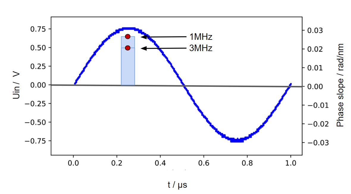
The presented method allows measurements of electronic processes with high spatial resolution. By combining a time-resolved electron holographic evaluation of the phase, conclusions can be drawn about the dynamic behavior of nanodevices and their causes, like capacitances. In this context, possible boundary effects, like surface or interface effects, can be investigated simultaneously by means of location-dependent measured value formation.
Ina Krüger
Technology Transfer Manager
+49 (0)30 314-75916
ina.krueger@tu-berlin.de
Technology validated in lab
pending: EP, US
approved: CN
Technische Universität Berlin
The Center for Intellectual Property (ZfgE) at the TU Berlin is the central point of contact for all topics relating to intellectual property law and intellectual property.
We patent and market the inventions of the TU Berlin, and we also teach and research technical and intellectual property law.
This makes us the central contact for inventors of the TU Berlin, for cooperation partners from industry and science as well as for interested scientists and experts from the fields of technology and law.
Zentrum für geistiges Eigentum
Technische Universität Berlin
Straße des 17. Juni 135
10623 Berlin